Nano Horizons Lab
CVD
Next generation materials
Since the discovery of graphene, people have been interested in two-dimensional materials due to their excellent properties, such as their outstanding catalytic ability, high transparency with high conductivity, and high electrical mobility at room temperature. However, scientists have drawn their attention away from graphene recently due to its major shortcoming of zero bandgap, which hinders its practical application. Therefore, scientists are dedicated to finding the next generation of the two-dimensional material, such as tellurene and transition metal dichalcogenides (TMDCs).
Our present works
In our present work, tellurene was synthesized on the SiO2/Si substrate via CVD process and is demonstrated for the first time. By controlling the ratio of the gas mixture, we can adjust the dimensions and thickness systematically. On the other hand, different from conventional synthesis methods only using TeO2, we also introduce TeCl4 as another precursor. By precisely controlling the ratio of TeO2/TeCl4, it is possible to manipulate the growth mechanism of tellurene from a one-dimensional nanowire to a two-dimensional tellurene.

Investigation of the gas ratio of Ar/H2 and the ratio of TeO2/TeCl4 precursors on the formation of tellurene

The reaction route of the formation of tellurene depending on the selection of precursors
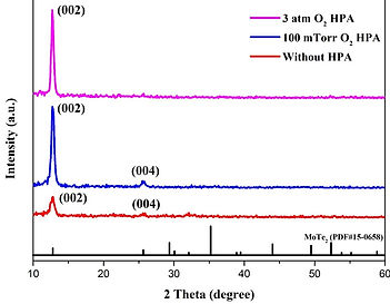
Besides, we adopt high pressure annealing (HPA) method to control the phases of MoTe2, Among two phases of MoTe2, 1T' MoTe2 is thermodynamically stable under a certain strain, while the 2H MoTe2 is stable under no strain. Therefore, we can utilize HPA to reduce the strain level of Mo film (grown by sputter). As an XRD result, the crystallinity of Mo thin film treated with HPA was improved significantly. On the other hand, the surface roughness of Mo film decreases from 1.18 nm to 0.889 nm.
In this situation, MoTe2 would prefer to present the 2H phase. In addition, with the aid of the selective HPA process, we can also synthesize 1T’/2H MoTe2 heterostructure in one step.

(a) Schematic diagram of the HPA treatment of Mo film (b) AFM image of Mo film without HPA treatment (c) AFM image of Mo film with HPA treatment

XRD spectra of Mo thin film under different pressure of annealing
Next, to examine the electrical transport properties of the synthesized 1T’/2H MoTe2 heterostructure, field effect transistors (FET) were fabricated. The 1T’ metallic phase can make the interface more like ohmic contact. Hence, inserting 1T’ MoTe2 between 2H MoTe2 and the electrode makes the mobility increase 6 times.
Our future works
PbI2 is a suitable material for UV-Vis photodetectors due to its direct band gap of 2.36 eV. If we can fabricate heterostructure photodetectors based on PbI2 and other materials, they can be self-powered. Besides the property of self-powered, there are still some characteristics of photodetectors that can be improved. For example, photodetectors can show wider potential applications (like wearable devices) if two-dimensional materials are grown on flexible polymer substrates.
However, one of the problems we face with wearable photodetectors is how to lower the growth temperature of two-dimensional materials. Since the polymer substrate will decompose when the growth temperature is too high. Thus, how to choose effective and low-temperature growth processes is very important.
The solution process is an effective and facile method to grow low-dimensional materials at low temperatures. For example, two-dimensional PbI2 can be grown on a flexible polymer substrate at 60 °C via a solution process. Thus, our goal is to fabricate heterostructure based on low-dimensional materials by low-temperature processes to make flexible, self-powered uv-vis photodetectors.

(a) PbI2 grown on ITO substrate by solution process (b) PbI2 grown on FTO substrate by solution process